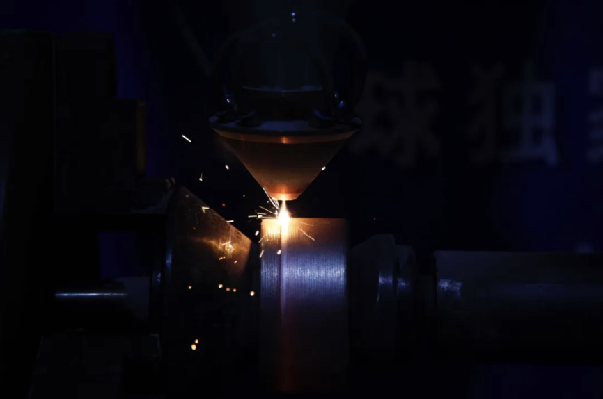
Exploratory application of picosecond lasers for cutting silicon carbide substrates
Substrate is the underlying material of semiconductor chips, which mainly plays the role of physical support, thermal conductivity and electrical conductivity. Silicon carbide has higher electrical conductivity and stronger thermal stability than traditional silicon materials, is one of the ideal materials for making high-temperature, high-frequency, high-power, high-voltage devices, which are widely used in solar energy, automotive components, charging piles, power supplies and other areas of life and production.
Silicon carbide substrate manufacturing needs to go through raw material synthesis, crystal growth, crystal cutting, wafer milling and processing, as well as cleaning, polishing, testing and many other links. Cutting link is one of the key links, due to the great hardness of silicon carbide, Mohs hardness of 9.5, and high brittleness, making the processing link cutting difficult, high breakage rate, some data show that the yield of silicon carbide processing link is about 70%, the cost accounted for about 50%. Therefore, the improvement of the cutting yield rate, help to reduce the cost of silicon carbide substrate manufacturing, but also in line with the semiconductor industry's expectations for cost reduction and efficiency of silicon carbide processing.
At present, the traditional cutting program of silicon carbide material is in the process of diamond wire cutting instead of mortar wire cutting, but there are still problems such as higher loss and higher cost of cutting consumables. Laser cutting, as an alternative to multi-wire cutting, has advantages in terms of accuracy, cutting efficiency, loss, product yield, etc., which helps to reduce the cost of silicon carbide, thus accelerating the penetration of finished products in the semiconductor market with silicon carbide as the substrate material.
Ultra-fast picosecond lasers with picosecond pulse widths are highly efficient tools for cutting silicon carbide substrate materials. Based on the market demand for laser cutting of silicon carbide substrate materials, Nuffy Optoelectronics has been extensively exploring laser cutting of silicon carbide with its self-developed picosecond laser as the light source. The pulse width of the picosecond laser is around 10ps, the beam quality is excellent (M² <1.3), and the pulse stability and power stability are very high, both less than 1% RMS. The ultra-high stability can provide a long-lasting and reliable output for the cutting process, which ensures the requirements of industrial-grade scenario cutting applications, as well as a higher consistency of the cutting to enhance the yield rate.
When the laser is applied to the silicon carbide material with a pulse duration on the order of picoseconds, as the pulse energy rises sharply, the ultra-high peak power can easily strip the outer layer of electrons, causing them to break away from the atomic bonds and form a plasma, and then material removal is realized, which is a cold processing process. The cold processing of picosecond laser is more friendly to the hard and brittle characteristics of silicon carbide, and it is less prone to chipping, as well as cracking when cutting. As the laser beam moves over the surface of the material, it forms a slit with a very narrow width, and completes the cutting of the material.
At the same time, the laser interaction time with the material is very short, only about 10 ps, the ions are ablated from the surface of the material before the energy is transferred to the surrounding material, and there is no thermal impact on the surrounding material, and the heat-affected zone is very small. And it is non-contact cutting, no mechanical stress, so that the high efficiency of silicon carbide cutting, small cutting seam, high material utilization, both reliable performance and cost advantages, can become an ideal alternative equipment for silicon carbide diamond wire cutting technology.
Large-size silicon carbide substrate can help realize cost reduction and efficiency, and has become a mainstream development trend. The larger the substrate size, the more chips can be produced per unit substrate, thus the lower the cost of the unit chip, while reducing the edge of the waste will further reduce the cost of chip production. According to media reports, the current global mainstream size of silicon carbide substrate 6 inches, is in transition to 8-inch substrate, the mainstream size of the domestic silicon carbide substrate is 4 inches and the transition to 6-inch substrate, is expected to 2025 ~ 2030 6-inch wafers in the domestic market demand will grow to 600,000 pieces. Larger size means higher processing difficulty, under the new situation in the new period, Nuffield Optoelectronics will be based on the current market demand for science and technology frontiers, step up scientific research and experimental exploration for the semiconductor industry breakthroughs in the development of empowerment.


Comments
Post a Comment